|
Project Name:
OPENCORES Application Board 1 (OAB1)
Introduction
As
you know, we have lots of free IP cores here, and we’ll have more coming soon.
We have to use these cores otherwise they are invaluable. For this reason the
idea of designing serials and open design boards are going to be available for
any designers around the world.
Objective
This
project is intended to:
-
To
design schematic can deal with analog signal and transport through Ethernet.
-
To
implementation CPU core and Ethernet core to one FPGA chip
-
To
program the necessary operation system and application software to achieve
the goal.
-
To
build the prototype board.
-
To
do the test for all functions.
Design
Flow
This
project can be divided into two parts. The board design and the cores design.
Anyone can use free or commercial tools to design and implement this project
Board
design flow can be done through four steps:
-
Block
Diagram design: I hope we use word 97+ for easy modify and exchange.
-
Schematic
entry: I will post schematic using PDF format. Anyone can also send me using
PDF, protel99se or Cadence format.
-
Layout
design: The final layout will use Allegro or Protel99se.
-
Board
implementation: This is the final step in the design where the designer
should work himself to produce his board unless we get funding or donation
from PCB manufactory.
Cores
design flow can be done through five steps:
-
Design
entry: Doesn’t matter the tools, we exchange only VHDL or Verilog codes.
-
Simulation:
I hope to use ModelSim or Active-HDL, but other tools also welcome.
-
Synthesis:
I hope to use FPGA express, but other tools also welcome.
-
Implementation:
I hope to use Xilinx FPGA.
-
Programming
Download: Using onboard parallel cable.
System
Description
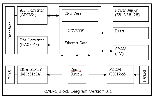
This
is the Board block diagram

The
system is composed of 5 main blocks:
Schematic Design
TBD
Layout Design
TBD
Current Status:
2001.8.20
Upload Board block diagram version 0.1
2001.8.21
Upload Board block diagram version 0.2
Maintainer(s):
Mailing-list:
cores@opencores.org_NOSPAM
References tools and links
Xscope
home page
SSM2141
Datasheet
DAC8248
Datasheet
AD7854
Datasheet
RTL8201
Datasheet
PE68515
Datasheet
Xilinx
Virtex-E Datasheet
Acknowledgment
|